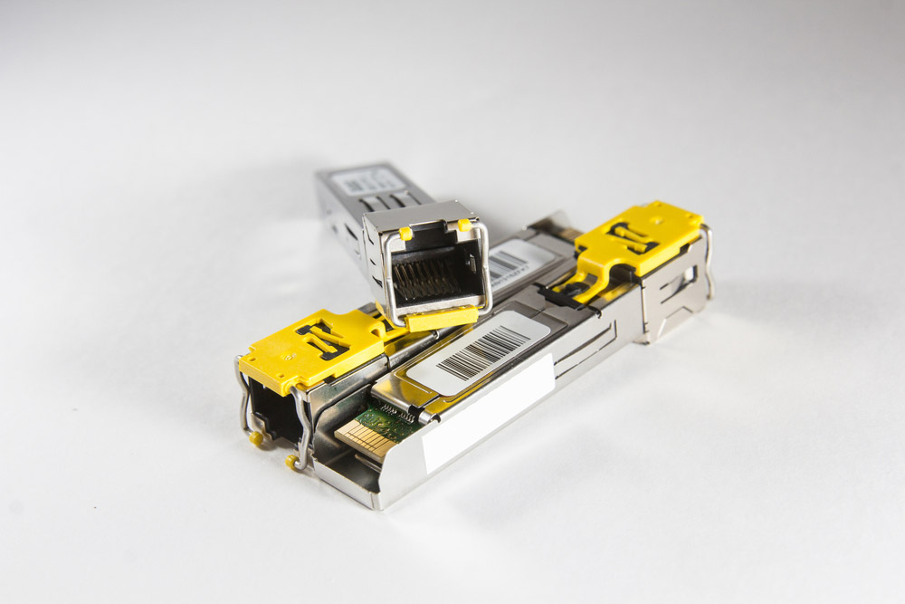
400G Optical Transceiver Optical Design and Testing

With the development of cloud computing and big data, optical modules, as the core components of optical interconnection, determine the quality level of the entire communication system. High-speed optical modules such as 100G QSFP28 and 400G QSFP-DD have become the development trend of the industry. This article will introduce the optical design and module testing of 400G optical modules.
Optical Design of Optical Module
Optical module placement and bonding finished products Driver and TIA use the placement machine to perform array placement according to the designed placement position marks to ensure that the position error accuracy of the two types of chip placement is less than 3 μm, so as to ensure the accuracy and optical quality of the product. coupling stability. After the driver and TIA finish the placement, the VCSEL laser chip and PD chip are placed so that they correspond to the working areas of the Driver and TIA respectively, and the marking is aligned according to the pin position of the GSG, and the placement error accuracy is less than 3 μm. After the placement is completed, set the parameters of the bonding machine according to the length and angle of the gold wire obtained in the simulation, and bond all the pins, and the bonding of the bare chip and the PCB is completed.
After the bonding is completed, this paper uses a high-precision coupling machine to perform active coupling on the module. The coupling work is divided into two times, one time to couple the Driver and TIA of a group of array patches, and use an optical power meter to detect the emitted optical power of the 4-channel TX. Use the software to detect the receiving responsivity of the 4-channel RX, and when the detection indicators of the transmission and reception reach the maximum value at the same time, the LENS is fixed by dispensing glue. The other group was coupled and fixed in the same manner.
Module Test
The eye diagram and BER test results of the 400G optical transceiver module produced in this paper show that the optical eye diagram is relatively clear without using forward error correction coding (FEC), and the jitter of the optical eye diagram is about 2.3 ps. It has good consistency and no bit error within 202 s. In addition, this paper also tests the system transmission performance of the 400G optical transceiver module at a transmission distance of 100 m. The eye diagram of each channel is not much different from the direct connection test results, the average jitter has increased, and the consistency of the eye diagram has not changed. Under the transmission rate of 50 Gb/s, there is still no packet loss, and the system performance is relatively stable. The total power of the entire optical module is 9.8 W, and the power consumption of the module is low.
Conclusion
In this paper, the 400G optical transceiver module modifies the parameters of DSP and Driver (including but not limited to the following registers: modulation current, bias current, pre-emphasis register, de-emphasis register, clock recovery equalization compensation parameters, etc.), to view the corresponding changes in the eye diagram Value, and finally get the optical eye diagram with the transmitted optical power above +1 dBm, the extinction ratio greater than 3 dB, and the TDECQ less than 2.0 dB; for the results of the optical eye diagram, use the self-loop method to self-loop the transmitting end and the receiving end of the optical module Connect, and conduct a bit error rate test, the bit error rate tested is less than 1E-12, which confirms the result that the eye diagram meets the transmission standard. The designed 400G optical transceiver module has a bit error rate of less than 1E-12 under the condition of a transmission distance of 100 m, and the total power of the module is 9.8 W, which meets the requirements of international standards.

